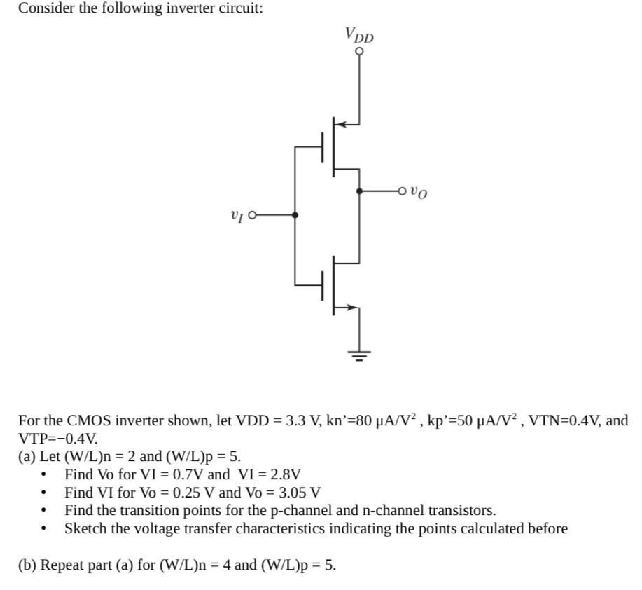
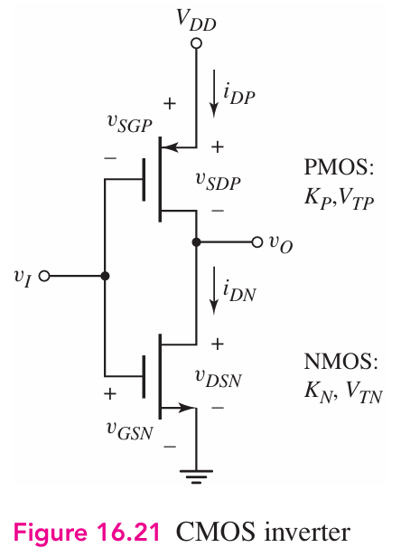
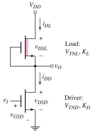
16.31 Consider the CMOS inverter in Figure 16.21 biased at VDD = 2.5 V. The transistor parameters are VTN = 0.4 V, VTP = −0.4 V, and Kn = Kp = 100 μA/V2. (a) Find the transition points for the p-channel and n− channel transistors. (b) Sketch the voltage transfer characteristics, including the appropriate voltage values at the transition points. (c) Determine vO for vI = 1.1 V and vI = 1.4 V. Figure 16.21 CMOS inverter


You'll get a detailed, step-by-step and expert verified solution.
 Work With Experts to Reach at Correct Answers