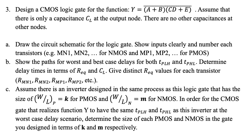
a) Draw the schematic for the circuit that implements F = x.(y + z + w) b) Using an inverter with Bn = Bp, as a sizing reference, determine the size of each transistor in this circuit that will equalize the nMOS and pMOS resistances. That is, specify size of each transistor (in terms of B) relative to Bn or Bp. c) If, rather than scaling transistor sizes as in part (b), we leave them all at Bn or p, identify the signal path (through which transistors) that will produce the slowest response (rise and fall).

You'll get a detailed, step-by-step and expert verified solution.
 Work With Experts to Reach at Correct Answers