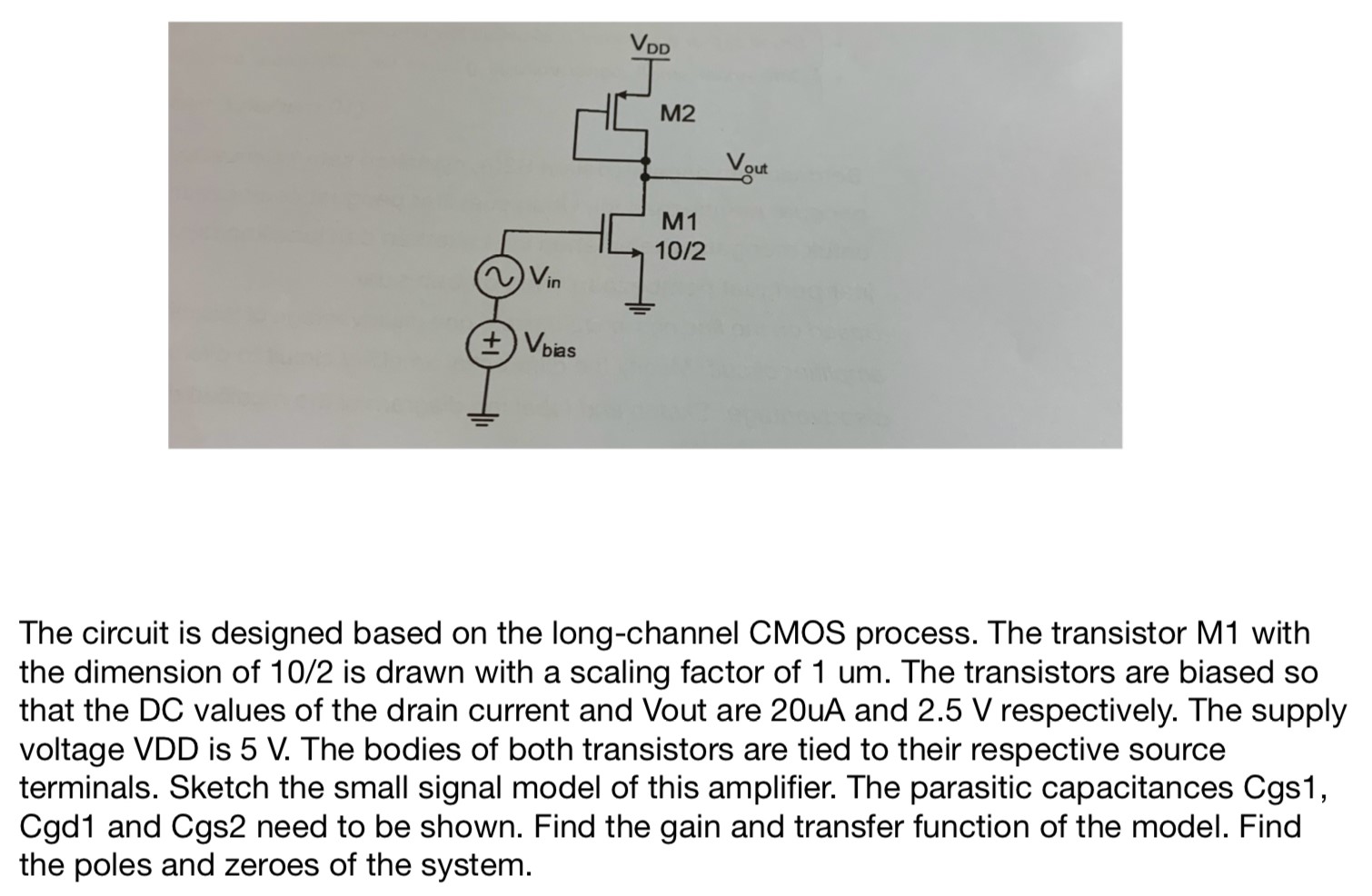
The circuit is designed based on the long-channel CMOS process. The transistor M1 with the dimension of 10/2 is drawn with a scaling factor of 1 um. The transistors are biased so that the DC values of the drain current and Vout are 20 uA and 2.5 V respectively. The supply voltage VDD is 5 V. The bodies of both transistors are tied to their respective source terminals. Sketch the small signal model of this amplifier. The parasitic capacitances Cgs1, Cgd1 and Cgs2 need to be shown. Find the gain and transfer function of the model. Find the poles and zeroes of the system.

![Figure P5-1 shows a common source single transistor MOSFET amplifier utilizing an N-Channel Enhancement Mode MOSFET. The term "common source" refers to the source terminal being shared by both the input circuit and the output circuit. The parameters for the MOSFET and the supply voltage are also given. Hand Analysis P1. In terms of DC bias, determine a value for VGS to set the drain current ID to 5 mA. Also determine a value for RD to set the VDS bias to 6 V. P2. In terms of small-signal parameters, determine the transconductance gm of this amplifier as well as the voltage gain, Av. P3. If vgs is a 0.1 Vpk sinewave at a frequency of 1 kHz [ie. vgs = 0.1sin(2pift)V ] determine an expression for the output voltage vOUT as a function of time. Sketch vIN and vOUT for two complete cycles, including the DC bias for each signal. Simulation P4. Simulate the circuit of Figure P5-1 to verify your hand analysis and create a plot similar to P3 as part of your prelab. Use the virtual MOSFET model in simulation with SPICE parameters VT0 = 1.8 V and KP = 120 mA/V2. (The default values of 100um for W and L will be fine since their ratio equals unity.)](https://www.doubtrix.com/js/ckeditor/filemanager/connectors/php/editor/1695874154-Avjhgifoih.png)