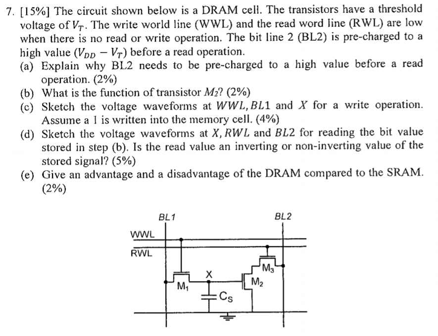
The circuit shown below is a DRAM cell. The transistors have a threshold voltage of VT. The write world line (WWL) and the read word line (RWL) are low when there is no read or write operation. The bit line 2 (BL2) is pre-charged to a high value (VDD−VT) before a read operation. (a) Explain why BL2 needs to be pre-charged to a high value before a read operation. (2%) (b) What is the function of transistor M2 ? (2%) (c) Sketch the voltage waveforms at WWL, BL1 and X for a write operation. Assume a 1 is written into the memory cell. (4%) (d) Sketch the voltage waveforms at X, RWL and BL2 for reading the bit value stored in step (b). Is the read value an inverting or non-inverting value of the stored signal? (5%) (e) Give an advantage and a disadvantage of the DRAM compared to the SRAM. (2%)
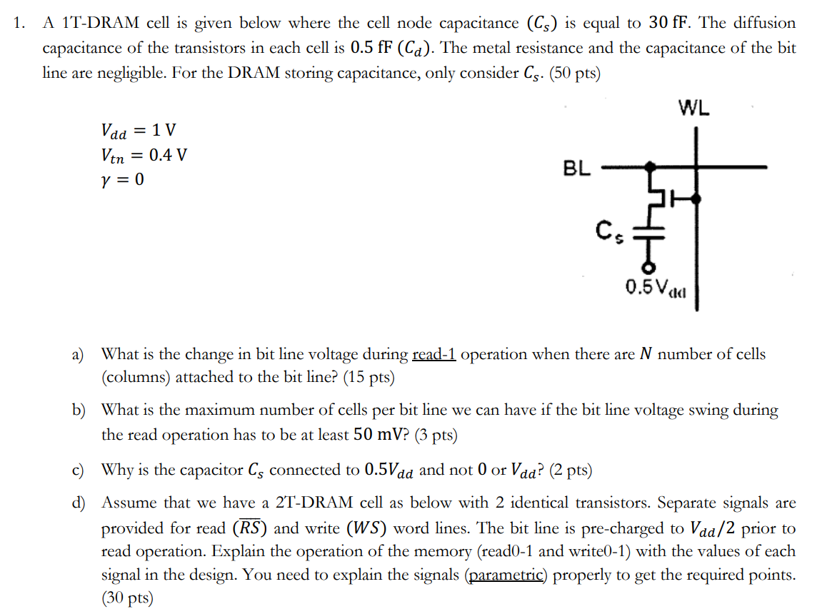
![[DRAM Analysis] Figure 4 shows a 1 μm×1 μm DRAM cell with NMOS width W = 0.5 μm and CS = 55 fF. Assume VDD = 1 V. Assume that for the NMOS transistor, CD = CG = 1 fF/μm, VTH = 0.2 V, Ileak, n = 1 nA for a W = 0.5 μm device. The cell is arranged in a 128×8 memory block and the wordline and bitline wires have a capacitance of CW = 0.2 fF/μm (i. e. 0.2 fF per unit length). Each bitline is connected to a sense amplifier with ΔVsense = 100 mV and input capacitance 5 fF, and you may ignore loading from any other peripheral circuitry. Use the ideal switch model for the transistor. Figure 4 (a) WRITE: Assume the cell initially stores a " 0 ". In order to write a "1", BL and WL are raised to VDD. What is the final value on node X ? (b) READ: After storing values in your memory, you pre-charge the bitline to VDD/2 and read. What is the final value on the bitline when you are reading a " 1 "?](https://www.doubtrix.com/uploads/editor/7753781189DiGpmnQIJq.png)