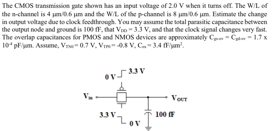
The CMOS transmission gate shown has an input voltage of 2.0 V when it turns off. The W/L of the n -channel is 4 μm/0.6 μm and the W/L of the p -channel is 8 μm/0.6 μm. Estimate the change in output voltage due to clock feedthrough. You may assume the total parasitic capacitance between the output node and ground is 100 fF, that VDD = 3.3 V, and that the clock signal changes very fast. The overlap capacitances for PMOS and NMOS devices are approximately Cgs-ov = Cgd-ov = 1.7 x 10⁻⁴ pF/μm. Assume, VTN0 = 0.7 V, VTP0 = −0.8 V, Cox = 3.4 fF/μm2.